
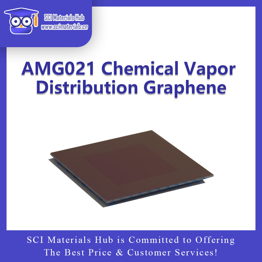
AMG021a CVD Graphene on Copper Foil
ACS Material is an industry-leading graphene on copper foil supplier. ACS Material produces high-quality, high-purity single- and multilayer graphene deposited on 35 μm copper foil via chemical vapor distribution (CVD). Our graphene films are continuous across the surface of the copper sheet on one or both sides. Standard sizes are 2”x2”, 4”x2”, and 6”x4”. Custom sizes are available upon request.
1. PREPARATION METHOD:CVD Method
2. WAFER STRUCTURE:
")
Graphene on Copper Foil (both sides)
")
Graphene on Copper Foil (Single-sided)
** Note: Copper Foil thickness is now 35μm now and if you need the old thickness of 45μm, please contact us for a quote.
** Standard products have graphene on both sides of the copper foil.
** ACS Material can provide Single-sided CVD Graphene on Copper as shown in the drop-down list. It is prepared by depositing PMMA on the graphene, etch away the graphene on the back side and then remove PMMA. Please note that there might be minor PMMA residues on the graphene surface and you can do a deeper cleaner if necessary. Please contact us if you have any questions or have other special requests.
** ACS Material can also provide large size Monolayer CVD Graphene on Copper (Graphene Factory) made by CVD Method and large size Monolayer CVD Graphene on SiO2/Si by Metal Assisted Exfoliation (MAE Process).
3. CHARACTERIZATION & ANALYSIS
Predominantly Single-layer Graphene on Copper Substrate
| Sheet Resistance | <600Ω/sq |
| Custom Order | <300Ω/sq |
| Transparency | >95% |
| Grain Size | ~50 μm |
ACS Material produces ultra-thin graphene on copper substrates using CVD. We then use PMMA method to transfer the copper-based graphene to a silicon substrate. Graphene on silicon substrate is available in four graphene thicknesses: 1 layer, 2 layers, 3-5 layers, and 6-8 layers. We offer 1cm x 1cm substrates and 1in x 1in substrates. We are also able to transfer graphene on these substrates using metal-assisted exfoliation (MEA) method. Please contact us today for details on our graphene on silicon substrate products.
Our exceptional graphene is suitable for all types of research. Graphene on silicon is paving the way to industrialization of graphene. All our CVD graphene samples conform to a stringent quality controls to ensure excellent consistency and reproducibility. We have single-, double-, and multilayer graphene sheets transferred onto silicon substrates. Research laboratories around the world trust ACS Material to provide the highest-quality graphene available on the market at the most reasonable prices. Shop ACS Material today.
| Sheet Resistance | <600Ω/sq |
| Custom Order | <300Ω/sq |
| Transparency | >95% |
Preparation Method:
Copper based graphene is prepared by CVD method.
Graphene is transferred from copper to silicon substrate.
.jpg)
Silicon Wafer:
Wafer Tickness: | 625 μm |
Resistivity: | <0.01 ohm-cm |
Type/Dopant: | P |
Orientation: | <100> |
Front Surface: | Polished |
Back Surface: | Etched |
AMG021c CVD Graphene on SiO2 Substrate
| Sheet Resistance | <600Ω/sq |
| Custom Order | <300Ω/sq |
| Transparency | >95% |
ACS Material is thrilled to be a part of the exciting research and innovation involving graphene. We are committed to providing a full range of outstanding graphene products, including these high-quality CVD Graphene sheets on SiO2 substrate. Our proven, proprietary method for CVD transfer of graphene onto P-type, 1-10 Ω·CM silicon dioxide substrate includes the following steps:
Growing monolayer graphene on copper foil
Depositing onto SiO2 via PMMA
Curing
Removing Cu by etching process
Washing PMMA/graphene in DI water
Redepositing PMMA/graphene onto silicon dioxide substrate followed by curing
Removing PMMA with acetone
The result is a superior product in every way.
Our process allows us to create graphene sheets in various sizes, from 0.5 cm x 0.5 cm to 1” x 1”.
Monolayer sheets or multilayer sheets are available: 1, 2, 3-5, or 6-8 layers.
The thickness and quality of the films is precisely controlled using Raman spectroscopy.
Graphene films are continuous with minimal holes and cracks.
CVD Graphene on SiO2 substrate is just one of many graphene products and services offered by ACS Material. Others include:
Large size graphene on copper foil in sheets up to 30 cm x 20 cm
Double or multilayer graphene sheets on various substrates
Pretreated graphene coated in PMMA; with simple steps? you can easily transfer graphene to other substrates
Graphical graphene customized according to graphics mask supplied by customers
Customized services providing different floors? different sizes of graphene, various graphene transfer services, nitrogen-doped graphene, etc; with ACS Material, you can get graphene products tailored to your research needs
AMG021d CVD Graphene on Si/SiO2 (Graphene Factory)
1. Preparation Method
CVD Method and Metal Assisted Exfoliation (MAE Process)
2. Characterizations
Monolayer CVD Graphene (Graphene Factory) | |
Transparency | > 97% |
Graphene Coverage | 100% with sporadic adlayers |
FET mobility* | >2700 cm2/ (V?s) |
Sheet resistance* | 430 ± 50 ?/sq |
Grain size | >40 μm |
Raman D/G ratio | Indistinguishable to 0.03 |
Si/SiO2 Substrate | |
| Type/Doping | P/B |
Wafer Thickness | 700 – 750 μm |
Oxide Thickness | 300 nm |
Resistivity | 1-25 (? -cm) |
Orientation | <1-0-0> |
Growth Method | CZ |
Metal Impurities | 1.00e10 – 5.00e10 (at/cm2)Substrate |
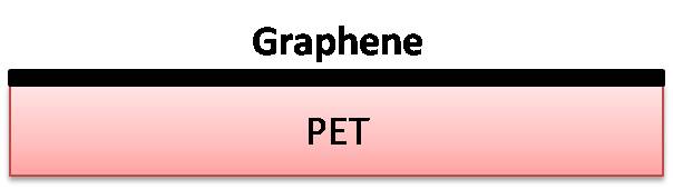
AMG021e CVD Graphene on PET Substrate
CVD graphene on PET is ideal for flexible and rigid touch screen display applications. Other possible applications include:
Energy electrodes, such as solar cells, batteries, fuel cells, and supercapacitors
Lightweight composite materials for automobile and aerospace industries
Heat dissipation for LED lighting
Gas and electromagnetic wave barriers
Biomedical applications
Transparent electrodes for flexible displays and touchscreens
All graphene samples from ACS Material are packaged and shipped carefully in order to minimize damage. Our rigorous quality standards and exceptional customer service mean you will get quality nanomaterials every time you shop with us. Call for more information today!
PET Substrate: ~188μm thick
| Sheet Resistance | <600Ω/sq |
| Custom Order | <300Ω/sq |
| Transparency | >95% |
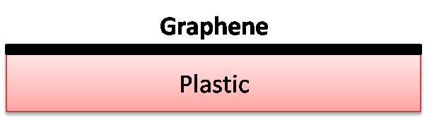
AMG021f CVD Graphene on Plastic Substrate
This Item Has Been Replaced By CVD Graphene On PET Substrate.
Description: Graphene transferred to Plastic substrate (a polymer mainly containing PET and other component (<10%)).
| Sheet Resistance | <600Ω/sq |
| Custom Order | <300Ω/sq |
| Transparency | >95% |
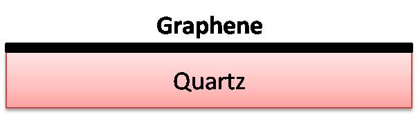
AMG021g CVD Graphene on Quartz Substrate
Quartz substrates have an advantage over other polished substrates because they offer significantly better light transmission rates and improved thermal resistance over alternatives such as glass. In addition, quartz has a high melting point and is chemically inert.
ACS Material supplies CVD graphene on quartz and other advanced graphene materials to the world’s leading research and development laboratories and universities. Advanced materials such as graphene are major players in the latest, most exciting innovations and ACS Material is proud to provide the tools that will make the future. Our wide product selection and low prices mean you won’t need to shop anywhere else for your graphene needs.
| Sheet Resistance | <600Ω/sq |
| Custom Order | <300Ω/sq |
| Transparency | >95% |
| CVD Graphene | Substrate |
| 1cm x 1cm | 15mm x 15mm, Thickness: 1mm* |
| 1inch x 1inch | 30mm x 30mm, Thickness: 1mm |
*ACS Material also offers plain quartz substrates in various sizes, please refer to our Quartz Substrate product page for more information. For customization options including CVD graphene transfer services to other size substrates or custom substrates, contact ACS Material today.
AMG021h CVD Graphene on Copper-PMMA Coated
Pretreated graphene is produced by applying PMMA to a copper substrate CVD graphene then removing the "reverse-side graphene". This form of graphene can then be used to study the transfer process by placing it directly in the ammonium persulphate solution to remove the copper followed by immersion in de-ionized water twice for cleaning. This method allows our customers to transfer to different substrates for their needs. A quicker alternative to this method is the ACS Material product Trivial Transfer Graphene?.
| Sheet Resistance | <600Ω/sq |
| Custom Order | <300Ω/sq |
| Transparency | >95% |
For international orders, please ask us for quotes via
Email: contact@scimaterials.cn
Tel: +86 153-5789-9751
Clik here to put quick orders on our Alibaba shop
AMG021 Chemical Vapor Distribution Graphene | |||
Product code | Product description | Price | Delivery date |
| 31021327-1 | CVD Graphene on Copper Foil(1layer,2"*2") | $437 | Ask for quote |
| 31021327-2 | CVD Graphene on Copper Foil(1layer,4"*2") | $779 | Ask for quote |
| 31021327-3 | CVD Graphene on Copper Foil(1layer,6"*4") | $1472 | Ask for quote |
| 31021327-4 | CVD Graphene on Copper Foil(1layer,12"*8") | $3650 | Ask for quote |
| 31021327-5 | CVD Graphene on Copper Foil(2layers,2"*2") | $437 | Ask for quote |
| 31021327-6 | CVD Graphene on Copper Foil(2layers,4"*2") | $779 | Ask for quote |
| 31021327-7 | CVD Graphene on Copper Foil(2layers,6"*4") | $1670 | Ask for quote |
| 31021327-8 | CVD Graphene on Copper Foil(3-5layers,2"*2") | $437 | Ask for quote |
| 31021327-9 | CVD Graphene on Copper Foil(3-5layers,4"*2") | $779 | Ask for quote |
| 31021327-10 | CVD Graphene on Copper Foil(3-5layers,6"*4") | $1670 | Ask for quote |
| 31021327-11 | CVD Graphene on Copper Foil(6-8layers,2"*2") | $437 | Ask for quote |
| 31021327-12 | CVD Graphene on Copper Foil(6-8layers,4"*2") | $779 | Ask for quote |
| 31021327-13 | CVD Graphene on Copper Foil(Graphene Factory, 1layer,4"*2") | $752 | Ask for quote |
| 31021328-1 | CVD Graphene on Silicon Substrate(1layer,1cm*1cm) | $200 | Ask for quote |
| 31021328-2 | CVD Graphene on Silicon Substrate(1layer,1"*1") | $275 | Ask for quote |
| 31021328-3 | CVD Graphene on Silicon Substrate(2layers,1cm*1cm) | $200 | Ask for quote |
| 31021328-4 | CVD Graphene on Silicon Substrate(2layers,1"*1") | $275 | Ask for quote |
| 31021328-5 | CVD Graphene on Silicon Substrate(3-5layers,1cm*1cm) | $200 | Ask for quote |
| 31021328-6 | CVD Graphene on Silicon Substrate(3-5layers,1"*1") | $275 | Ask for quote |
| 31021328-7 | CVD Graphene on Silicon Substrate(6-8layers,1cm*1cm) | $200 | Ask for quote |
| 31021328-8 | CVD Graphene on Silicon Substrate(6-8layers,1"*1") | $275 | Ask for quote |
| 31021329-1 | CVD Graphene on SiO2 Substrate(1layer,0.5cm*0.5cm) | $200 | Ask for quote |
| 31021329-2 | CVD Graphene on SiO2 Substrate(1layer,1cm*1cm) | $275 | Ask for quote |
| 31021329-3 | CVD Graphene on SiO2 Substrate(1layer,3cm*3cm) | $302 | Ask for quote |
| 31021329-4 | CVD Graphene on SiO2 Substrate(1layer,7cm*7cm) | $1202 | Ask for quote |
| 31021329-5 | CVD Graphene on SiO2 Substrate(1layer,1"*1") | $275 | Ask for quote |
| 31021329-6 | CVD Graphene on SiO2 Substrate(2layers,1cm*1cm) | $200 | Ask for quote |
| 31021329-7 | CVD Graphene on SiO2 Substrate(2layers,3cm*3cm) | $302 | Ask for quote |
| 31021329-8 | CVD Graphene on SiO2 Substrate(2layers,7cm*7cm) | $1202 | Ask for quote |
| 31021329-9 | CVD Graphene on SiO2 Substrate(2layers,1"*1") | $275 | Ask for quote |
| 31021329-10 | CVD Graphene on SiO2 Substrate(3-5layers,1cm*1cm) | $200 | Ask for quote |
| 31021329-11 | CVD Graphene on SiO2 Substrate(3-5layers,3cm*3cm) | $302 | Ask for quote |
| 31021329-12 | CVD Graphene on SiO2 Substrate(3-5layers,7cm*7cm) | $1202 | Ask for quote |
| 31021329-13 | CVD Graphene on SiO2 Substrate(3-5layers,1"*1") | $275 | Ask for quote |
| 31021329-14 | CVD Graphene on SiO2 Substrate(6-8layers,1cm*1cm) | $200 | Ask for quote |
| 31021329-15 | CVD Graphene on SiO2 Substrate((6-8layers,3cm*3cm) | $302 | Ask for quote |
| 31021329-16 | CVD Graphene on SiO2 Substrate((6-8layers,7cm*7cm) | $1202 | Ask for quote |
| 31021329-17 | CVD Graphene on SiO2 Substrate(6-8layers,1"*1") | $275 | Ask for quote |
| 3102130-1 | CVD Graphene on Si/SiO2 (Graphene Factory,6inch) | $1409 | Ask for quote |
| 3102130-2 | CVD Graphene on Si/SiO2 (Graphene Factory,8inch) | $2255 | Ask for quote |
| 31021331-1 | CVD Graphene on PET Substrate(1layer,1cm*1cm) | $200 | Ask for quote |
| 31021331-2 | CVD Graphene on PET Substrate(1layer,10cm*5cm) | $1004 | Ask for quote |
| 31021331-3 | CVD Graphene on PET Substrate(1layer,2"*2") | $509 | Ask for quote |
| 31021331-4 | CVD Graphene on PET Substrate(1layer,12"*8") | $3650 | Ask for quote |
| 31021331-5 | CVD Graphene on PET Substrate(2layers,1cm*1cm) | $200 | Ask for quote |
| 31021331-6 | CVD Graphene on PET Substrate(2layers,10cm*5cm) | $1004 | Ask for quote |
| 31021331-7 | CVD Graphene on PET Substrate(2layers,2"*2") | $509 | Ask for quote |
| 31021331-8 | CVD Graphene on PET Substrate(3-5layers,1cm*1cm) | $200 | Ask for quote |
| 31021331-9 | CVD Graphene on PET Substrate(3-5layers,10cm*5cm) | $1004 | Ask for quote |
| 31021331-10 | CVD Graphene on PET Substrate(3-5layers,2"*2") | $509 | Ask for quote |
| 31021331-11 | CVD Graphene on PET Substrate(6-8layers,1cm*1cm) | $200 | Ask for quote |
| 31021331-12 | CVD Graphene on PET Substrate(6-8layers,10cm*5cm) | $1004 | Ask for quote |
| 31021331-13 | CVD Graphene on PET Substrate(6-8layers,2"*2") | $509 | Ask for quote |
| 31021332-1 | CVD Graphene on Plastic Substrate(1layer,10cm*5cm) | $1004 | Ask for quote |
| 31021333-1 | CVD Graphene on Quartz Substrate(1layer,1cm*1cm) | $200 | Ask for quote |
| 31021333-2 | CVD Graphene on Quartz Substrate(1layer,1"*1") | $275 | Ask for quote |
| 31021333-3 | CVD Graphene on Quartz Substrate(2layers,1cm*1cm) | $200 | Ask for quote |
| 31021333-4 | CVD Graphene on Quartz Substrate(2layers,1"*1") | $302 | Ask for quote |
| 31021333-5 | CVD Graphene on Quartz Substrate(3-5layers,1cm*1cm) | $200 | Ask for quote |
| 31021333-6 | CVD Graphene on Quartz Substrate(3-5layers,1"*1") | $302 | Ask for quote |
| 31021333-7 | CVD Graphene on Quartz Substrate(6-8layers,1cm*1cm) | $200 | Ask for quote |
| 31021333-8 | CVD Graphene on Quartz Substrate(6-8layers,1"*1") | $302 | Ask for quote |
| 31021334-1 | CVD Graphene on Copper-PMMA Coated(1layer,1cm*1cm) | $200 | Ask for quote |
| 31021334-2 | CVD Graphene on Copper-PMMA Coated(2layers,1cm*1cm) | $200 | Ask for quote |
| 31021334-3 | CVD Graphene on Copper-PMMA Coated(3-5layers,1cm*1cm) | $200 | Ask for quote |
| 31021334-4 | CVD Graphene on Copper-PMMA Coated(6-8layers,1cm*1cm) | $200 | Ask for quote |
| 31021334-5 | CVD Graphene on Copper-PMMA Coated(1layer,2"*2") | $716 | Ask for quote |
| 31021334-6 | CVD Graphene on Copper-PMMA Coated(2layers,2"*2") | $716 | Ask for quote |
| 31021334-7 | CVD Graphene on Copper-PMMA Coated(3-5layers,2"*2") | $716 | Ask for quote |
| 31021334-8 | CVD Graphene on Copper-PMMA Coated(6-8layers,2"*2") | $716 | Ask for quote |
| 31021334-9 | CVD Graphene on Copper-PMMA Coated(2layers,4"*2") | $1085 | Ask for quote |
| SCI Materials Hub is Committed to Offering The Best Price & Customer Services! | |||
- The price listed above is in U.S. dollars
Worldwide shipping via DHL, SF-Express, FedEx, TNT & other requested carriers.
Payments via Bank Transfer, Paypal, Credit card (via Alibaba), Alipay, Wechat-pay are accepted.
Please contact us for larger quantities or becoming our distributors.
Partial references citing our materials (from Google Scholar)

Carbon Dioxide Reduction
1. ACS Nano Strain Relaxation in Metal Alloy Catalysts Steers the Product Selectivity of Electrocatalytic CO2 Reduction
The bipolar membrane (Fumasep FBM) in this paper was purchased from SCI Materials Hub, which was used in rechargeable Zn-CO2 battery tests. The authors reported a strain relaxation strategy to determine lattice strains in bimetal MNi alloys (M = Pd, Ag, and Au) and realized an outstanding CO2-to-CO Faradaic efficiency of 96.6% with outstanding activity and durability toward a Zn-CO2 battery.
2. Front. Chem. Boosting Electrochemical Carbon Dioxide Reduction on Atomically Dispersed Nickel Catalyst
In this paper, Vulcan XC-72R was purchased from SCI Materials Hub. Vulcan XC 72R carbon is the most common catalyst support used in the anode and cathode electrodes of Polymer Electrolyte Membrane Fuel Cells (PEMFC), Direct Methanol Fuel Cells (DMFC), Alkaline Fuel Cells (AFC), Microbial Fuel Cells (MFC), Phosphoric Acid Fuel Cells (PAFC), and many more!
3. Adv. Mater. Partially Nitrided Ni Nanoclusters Achieve Energy-Efficient Electrocatalytic CO2 Reduction to CO at Ultralow Overpotential
An AEM membrane (Sustainion X37-50 Grade RT, purchased from SCI Materials Hub) was activated in 1 M KOH for 24 h, washed with ultra-purity water prior to use.
4. Adv. Funct. Mater. Nanoconfined Molecular Catalysts in Integrated Gas Diffusion Electrodes for High-Current-Density CO2 Electroreduction
In this paper (Supporting Information), an anion exchanged membrane (Fumasep FAB-PK-130 obtained from SCI Materials Hub (www.scimaterials.cn)) was used to separate the catholyte and anolyte chambers.
SCI Materials Hub: we also recommend our Fumasep FAB-PK-75 for the use in a flow cell.
5. Appl. Catal. B Efficient utilization of nickel single atoms for CO2 electroreduction by constructing 3D interconnected nitrogen-doped carbon tube network
In this paper, the Nafion 117 membrane was obtained from SCI Materials Hub.
In this paper, Proton exchange membrane (Nafion 117), Nafion D520, and Toray 060 carbon paper were purchased from SCI Materials Hub.
7. National Science Review Confinement of ionomer for electrocatalytic CO2 reduction reaction via efficient mass transfer pathways
An anion exchange membrane (PiperION-A15-HCO3) was obtained from SCI Materials Hub.
8. Catalysis Communications Facilitating CO2 electroreduction to C2H4 through facile regulating {100} & {111} grain boundary of Cu2O
Carbon paper (TGPH060), membrane solution (Nafion D520), and ionic membrane (Nafion N117) were obtained from Wuhu Eryi Material Technology Co., Ltd (a company under SCI Materials Hub).
Batteries
1. J. Mater. Chem. A Blocking polysulfides with a Janus Fe3C/N-CNF@RGO electrode via physiochemical confinement and catalytic conversion for high-performance lithium–sulfur batteries
Graphene oxide (GO) in this paper was obtained from SCI Materials Hub. The authors introduced a Janus Fe3C/N-CNF@RGO electrode consisting of 1D Fe3C decorated N-doped carbon nanofibers (Fe3C/N-CNFs) side and 2D reduced graphene oxide (RGO) side as the free-standing carrier of Li2S6 catholyte to improve the overall electrochemical performance of Li-S batteries.
This paper used more than 10 kinds of materials from SCI Materials Hub and the authors gave detailed properity comparsion.
The commercial IEMs of Fumasep FAB-PK-130 and Nafion N117 were obtained from SCI Materials Hub.
Gas diffusion layers of GDL340 (CeTech) and SGL39BC (Sigracet) and Nafion dispersion (Nafion D520) were obtained from SCI Materials Hub.
Zn foil (100 mm thickness) and Zn powder were obtained from the SCI Materials Hub.
Commercial 20% Pt/C, 40% Pt/C and IrO2 catalysts were also obtained from SCI Materials Hub.
3. Journal of Energy Chemistry Vanadium oxide nanospheres encapsulated in N-doped carbon nanofibers with morphology and defect dual-engineering toward advanced aqueous zinc-ion batteries
In this paper, carbon cloth (W0S1011) was obtained from SCI Materials Hub. The flexible carbon cloth matrix guaranteed the stabilization of the electrode and improved the conductivity of the cathode.
4. Energy Storage Materials Defect-abundant commercializable 3D carbon papers for fabricating composite Li anode with high loading and long life
The 3D carbon paper (TGPH060 raw paper) were purchased from SCI Materials Hub.
5. Nanomaterials A Stable Rechargeable Aqueous Zn–Air Battery Enabled by Heterogeneous MoS2 Cathode Catalysts
Nafion D520 (5 wt%), and carbon paper (GDL340) were received from SCI-Materials-Hub.
Carbon cloth (W0S1011) and other electrochemical consumables required for air cathode were provided by SCI Materials Hub.
Oxygen Reduction Reaction
1. J. Chem. Eng. Superior Efficiency Hydrogen Peroxide Production in Acidic Media through Epoxy Group Adjacent to Co-O/C Active Centers on Carbon Black
In this paper, Vulcan XC 72 carbon black, ion membrane (Nafion N115, 127 μL), Nafion solution (D520, 5 wt%), and carbon paper (AvCarb GDS 2230 and Spectracarb 2050A-1050) were purchased from SCI Materials Hub.
2. Journal of Colloid and Interface Science Gaining insight into the impact of electronic property and interface electrostatic field on ORR kinetics in alloy engineering via theoretical prognostication and experimental validation
The 20 wt% Pt3M (M = Cr, Co, Cu, Pd, Sn, and Ir) were purchased from SCI Materials Hub. This work places emphasis on the kinetics of the ORR concerning Pt3M (M = Cr, Co, Cu, Pd, Sn, and Ir) catalysts, and integrates theoretical prognostication and experimental validation to illuminate the fundamental principles of alloy engineering.
Water Electrolysis
1. International Journal of Hydrogen Energy Gold as an efficient hydrogen isotope separation catalyst in proton exchange membrane water electrolysis
The cathodic catalysts of Pt/C (20 wt%, 2–3 nm) and Au/C (20 wt%, 4–5 nm) were purchased from SCI Materials Hub.
2. Small Science Silver Compositing Boosts Water Electrolysis Activity and Durability of RuO2 in a Proton-Exchange-Membrane Water Electrolyzer
Two fiber felts (0.35 mm thickness, SCI Materials Hub) were used as the porous transport layers at both the cathode and the anode.
3. Advanced Functional Materials Hierarchical Crystalline/Amorphous Heterostructure MoNi/NiMoOx for Electrochemical Hydrogen Evolution with Industry-Level Activity and Stability
Anion-exchange membrane (FAA-3-PK-130) was obtained from SCI Materials Hub website.
Fuel Cells
1. Polymer Sub-two-micron ultrathin proton exchange membrane with reinforced mechanical strength
Gas diffusion electrode (60% Pt/C, Carbon paper) was purchased from SCI Materials Hub.
Characterization
1. Chemical Engineering Journal Electrochemical reconstitution of Prussian blue analogue for coupling furfural electro-oxidation with photo-assisted hydrogen evolution reaction
An Au nanoparticle film was deposited on the total reflecting plane of a single reflection ATR crystal (SCI Materials Hub, Wuhu, China) via sputter coater.

|
We Provide A Broad Range of Materials, Instruments & Solutions in Advanced Science and Technologies | About Us |