
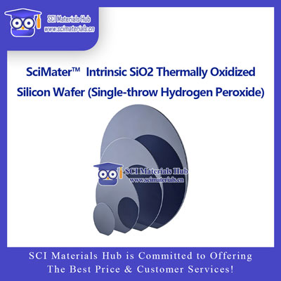
Intrinsic monocrystalline silicon substrates with dense thermally grown SiO₂ layers for 2D-material devices, electrical testing, dielectric studies, thin-film deposition, micro-/nanofabrication, surface modification, and low-background-current experiments. Single-side and double-side oxide structures are available, with common oxide thicknesses of 100 nm, 285 nm, and 300 nm.
SciMater™ Intrinsic SiO₂ Thermal Oxide Silicon Wafers use intrinsic monocrystalline silicon as the base substrate. A dense silicon dioxide layer is grown directly on the silicon surface through high-temperature dry oxidation, wet oxidation, or a combined thermal-oxidation process. The in-situ-grown oxide forms a tightly bonded interface with the silicon and can function as an electrical insulation layer, dielectric layer, protective layer, surface-functional layer, or optical interference layer.
Intrinsic silicon has a relatively low free-carrier concentration and can reduce substrate-related interference in low-leakage, electrical, dielectric, and RF measurements. The principal product structures are SSP single-side oxide and SSP double-side oxide. Crystal orientation, resistivity, wafer thickness, oxide thickness, and tolerances are subject to the confirmed order or corresponding batch documentation.
Low free-carrier background for low-current, electrical, RF, dielectric, and interface studies.
Dense and uniform oxide with a strongly bonded and stable silicon/oxide interface.
Single-side oxide supports front-side processing; double-side oxide provides insulation and protection on both surfaces.
Standard options include 100 nm, 285 nm, and 300 nm; other thicknesses may be confirmed.
Suitable for field-effect devices, dielectric tests, microelectrodes, and low-current sensor research.
285 nm and 300 nm oxide layers support locating and observing graphene and other 2D materials.
Square, rectangular, circular, mechanical-diced, and laser-scribed formats can be evaluated.
Orientation, resistivity, thickness, tolerances, packaging, and batch inspection documents may be specified.
The table below compares intrinsic SSP single-side oxide and intrinsic SSP double-side oxide wafers.
| Comparison Item | Intrinsic SSP Single-Side Oxide Wafer | Intrinsic SSP Double-Side Oxide Wafer |
|---|---|---|
| Substrate Material | Intrinsic monocrystalline silicon | Intrinsic monocrystalline silicon |
| Polishing | Precision single-side polished | Precision single-side polished |
| Oxide Structure | Single-side oxide on the primary functional surface | Thermal oxide layers on both front and back surfaces |
| Common Oxide Thicknesses | 100 nm, 285 nm, and 300 nm | 100 nm, 285 nm, and 300 nm |
| Other Oxide Thicknesses | Subject to wafer size and batch availability | Subject to wafer size and batch availability |
| Common Full-Wafer Size | 4 inch; other sizes available upon inquiry | 4 inch; other sizes available upon inquiry |
| Crystal Orientation | <100>or<111>, subject to order confirmation | <100>or<111>, subject to order confirmation |
| Conductivity Type | Intrinsic undoped or high-resistivity specification | Intrinsic undoped or high-resistivity specification |
| Resistivity | Confirmed by order or batch documentation | Confirmed by order or batch documentation |
| Back-Surface Condition | No target oxide layer or batch-specific process condition | Back surface contains a thermally grown SiO₂ layer |
| Main Advantage | Simple structure, clear front-side process surface, and relatively lower cost | Double-side insulation, double-side protection, and reduced back-side conduction effects |
| Recommended Applications | 2D materials, thin-film deposition, surface modification, and front-side device processing | Low-leakage testing, dielectric studies, RF research, and double-side insulated device structures |
| Cutting Services | Square, circular, and customized cut pieces | Square, circular, and customized cut pieces |
| Packaging | Wafer box, single-wafer box, clean bag, or customized packaging | Wafer box, single-wafer box, clean bag, or customized packaging |
Not every wafer size is available with every oxide thickness. Confirm wafer thickness, resistivity, oxide-thickness tolerance, TTV, Bow, Warp, and surface requirements before ordering.
For transfer, alignment, optical identification, and device fabrication using graphene, MoS₂, MXene, and other 2D materials.
Suitable for low-leakage measurements, dielectric characterization, capacitor structures, microelectrodes, and electrical-device research.
Compatible with evaporation, sputtering, CVD, ALD, spin coating, and solution-based film preparation.
Suitable for photolithography, etching, pattern transfer, electrical isolation, and micro-/nanodevice process verification.
Intrinsic or high-resistivity silicon can reduce the influence of substrate conduction on RF and dielectric measurements.
Suitable for silanization, hydrophilic/hydrophobic treatment, molecular functionalization, biointerfaces, and surface chemistry.
Useful as an insulating base substrate for gas, biological, electrochemical, and miniature sensors.
Suitable for semiconductor processing, 2D materials, thin-film analysis, and microfabrication education.
Confirm dimensions, oxide structure, oxide thickness, orientation, resistivity, and quantity.
Use the label and order information to identify the single-side oxide, double-side oxide, and primary polished surface.
Wear powder-free gloves and use wafer tweezers or a vacuum wand to handle the edge region.
Use clean nitrogen first and apply a compatible cleaning procedure when necessary.
Confirm fixture compatibility and avoid edge stress, vacuum-chuck marks, or local bending.
Set suitable conditions for transfer, deposition, photolithography, etching, or electrical testing.
Select a cleaning method that does not significantly etch or damage the SiO₂ layer.
After cleaning and drying, return the wafer to a wafer box or clean sample case and retain the batch information.
| Item | Recommendation | Key Precaution |
|---|---|---|
| Particle Cleaning | Use clean nitrogen or deionized-water rinsing first | Avoid dragging hard particles across the functional surface |
| Organic Contamination | Select a process-compatible organic solvent | Prevent solvent residue after cleaning |
| Fluoride Systems | Evaluate material compatibility before use | HF and other fluoride-containing solutions etch SiO₂ |
| Strong Alkalis | Control concentration, temperature, and treatment time | Some strong alkalis can affect both the oxide and silicon substrate |
| Surface Protection | Handle only the edge or a non-critical region | Avoid contact with fingers, sharp tweezers, and paper fibers |
| Storage Environment | Clean, dry, low-particle, and away from corrosive gases | A clean dry cabinet is recommended |
| Packaging | Keep in the original wafer box, single-wafer box, or clean bag | Use spacers between wafers to prevent surface rubbing |
| Opened Packages | Use promptly and reseal unused products | Record the batch, opening date, and intended experiment |
It uses intrinsic monocrystalline silicon as the substrate, with an SiO₂ layer grown directly on the silicon surface by high-temperature thermal oxidation. The intrinsic substrate has a relatively low carrier concentration and is useful for experiments sensitive to substrate conduction.
An SSP single-side oxide wafer has the oxide layer on the principal functional surface and is suitable for front-side processing. An SSP double-side oxide wafer has oxide layers on both surfaces for double-side insulation, protection, and process isolation.
Intrinsic silicon generally has a lower dopant concentration and lower carrier background, making it suitable for low-leakage, electrical, dielectric, and RF studies. The actual resistivity must still be confirmed by batch.
They are commonly used for transfer, positioning, and optical observation of graphene, MoS₂, and other 2D materials, and they are also suitable for micro-/nanofabrication, thin-film deposition, and general insulation.
Yes. Before use, perform particle cleaning, dehydration, and surface pretreatment according to the process, and verify oxide thickness and fixture compatibility.
HF and other fluoride-containing solutions can significantly etch SiO₂, and some strong alkaline systems may also affect it. Confirm concentration, temperature, treatment time, and material compatibility before use.
Customization can be evaluated according to wafer size, oxide structure, target thickness, allowed tolerance, and quantity. Square, rectangular, circular, and laser-scribed formats can also be confirmed.
Confirm single- or double-side oxide, full wafer or cut piece, dimensions, oxide thickness, crystal orientation, resistivity, wafer thickness, quantity, tolerances, and packaging requirements.
SciMater™ Intrinsic SiO₂ Thermal Oxide Silicon Wafers are available in SSP single-side oxide and SSP double-side oxide structures. The combination of an intrinsic monocrystalline silicon substrate and a dense thermally grown SiO₂ layer is suitable for 2D-material devices, low-leakage measurements, dielectric research, thin-film deposition, micro-/nanofabrication, sensors, and surface studies. Product selection should focus on the number of oxide surfaces, oxide thickness, crystal orientation, resistivity, wafer size, and cutting format.
Covers intrinsic SSP double-side oxide and intrinsic DSP double-side oxide silicon wafers and cut pieces. All prices are shown in USD.
| Oxide System | Product Form | Size | Oxide Thickness / Specification | N-Type Intrinsic Oxide Silicon | P-Type Intrinsic Oxide Silicon | ||||
|---|---|---|---|---|---|---|---|---|---|
| <100> | <110> | <111> | <100> | <110> | <111> | ||||
| Intrinsic SSP Double-Side Oxide Specifications | |||||||||
| Intrinsic SSP Double-Side Oxide Intrinsic Silicon · Single-Side Polished · Double-Side Oxidized Square pieces, circular pieces, processed wafers, and 2–8 inch intrinsic double-side oxide silicon wafers. | Cut Piece | 5 × 5 mm | 300 nm | $8 | $8 | $8 | $8 | $8 | $8 |
| Cut Piece | Ø10 mm | 300 nm | $10 | $10 | $10 | $10 | $10 | $10 | |
| Cut Piece | 10 × 10 mm | 300 nm | $10 | $10 | $10 | $10 | $10 | $10 | |
| Cut Piece | Ø15 mm | 300 nm | $14 | $14 | $14 | $14 | $14 | $14 | |
| Cut Piece | 15 × 15 mm | 300 nm | $14 | $14 | $14 | $14 | $14 | $14 | |
| Cut Piece | Ø20 mm | 300 nm | $17 | $17 | $17 | $17 | $17 | $17 | |
| Cut Piece | 20 × 20 mm | 300 nm | $17 | $17 | $17 | $17 | $17 | $17 | |
| Full Wafer | 2 Inch | 285 nm | $60 | $60 | $60 | $60 | $60 | $60 | |
| Full Wafer | 3 Inch | 285 nm | $108 | $108 | $108 | $108 | $108 | $108 | |
| Full Wafer | 4 Inch | 10 nm | $130 | $130 | $130 | $130 | $130 | $130 | |
| Full Wafer | 4 Inch | 20 nm | $108 | $108 | $108 | $108 | $108 | $108 | |
| Full Wafer | 4 Inch | 50–2000 nm | $84 | $84 | $84 | $84 | $84 | $84 | |
| Full Wafer | 4 Inch | 7 μm | $340 | $340 | $340 | $340 | $340 | $340 | |
| Processed Wafer | 4 Inch | Approx. 55 SSP Pieces, 10 × 10 mm Laser-Scribed | $103 | $103 | $103 | $103 | $103 | $103 | |
| Processed Wafer | 4 Inch | Approx. 60 SSP Pieces, 10 × 10 mm Diced | $116 | $116 | $116 | $116 | $116 | $116 | |
| Full Wafer | 5 Inch | 5 μm | $228 | $228 | $228 | $228 | $228 | $228 | |
| Full Wafer | 6 Inch | 3 μm | $340 | $340 | $340 | $340 | $340 | $340 | |
| Full Wafer | 8 Inch | 285 nm | $244 | $244 | $244 | $244 | $244 | $244 | |
| Intrinsic DSP Double-Side Oxide Specifications | |||||||||
| Intrinsic DSP Double-Side Oxide Intrinsic Silicon · Double-Side Polished · Double-Side Oxidized Intrinsic double-side-polished, double-side-oxidized circular silicon pieces. | Circular Piece | Ø10 mm | 7 μm | $40 | $40 | $40 | $40 | $40 | $40 |
Partial references citing our materials (from Google Scholar)

Carbon Dioxide Reduction
1. ACS Nano Strain Relaxation in Metal Alloy Catalysts Steers the Product Selectivity of Electrocatalytic CO2 Reduction
The bipolar membrane (Fumasep FBM) in this paper was purchased from SCI Materials Hub, which was used in rechargeable Zn-CO2 battery tests. The authors reported a strain relaxation strategy to determine lattice strains in bimetal MNi alloys (M = Pd, Ag, and Au) and realized an outstanding CO2-to-CO Faradaic efficiency of 96.6% with outstanding activity and durability toward a Zn-CO2 battery.
2. Front. Chem. Boosting Electrochemical Carbon Dioxide Reduction on Atomically Dispersed Nickel Catalyst
In this paper, Vulcan XC-72R was purchased from SCI Materials Hub. Vulcan XC 72R carbon is the most common catalyst support used in the anode and cathode electrodes of Polymer Electrolyte Membrane Fuel Cells (PEMFC), Direct Methanol Fuel Cells (DMFC), Alkaline Fuel Cells (AFC), Microbial Fuel Cells (MFC), Phosphoric Acid Fuel Cells (PAFC), and many more!
3. Adv. Mater. Partially Nitrided Ni Nanoclusters Achieve Energy-Efficient Electrocatalytic CO2 Reduction to CO at Ultralow Overpotential
An AEM membrane (Sustainion X37-50 Grade RT, purchased from SCI Materials Hub) was activated in 1 M KOH for 24 h, washed with ultra-purity water prior to use.
4. Adv. Funct. Mater. Nanoconfined Molecular Catalysts in Integrated Gas Diffusion Electrodes for High-Current-Density CO2 Electroreduction
In this paper (Supporting Information), an anion exchanged membrane (Fumasep FAB-PK-130 obtained from SCI Materials Hub (www.scimaterials.cn)) was used to separate the catholyte and anolyte chambers.
SCI Materials Hub: we also recommend our Fumasep FAB-PK-75 for the use in a flow cell.
5. Appl. Catal. B Efficient utilization of nickel single atoms for CO2 electroreduction by constructing 3D interconnected nitrogen-doped carbon tube network
In this paper, the Nafion 117 membrane was obtained from SCI Materials Hub.
In this paper, Proton exchange membrane (Nafion 117), Nafion D520, and Toray 060 carbon paper were purchased from SCI Materials Hub.
7. National Science Review Confinement of ionomer for electrocatalytic CO2 reduction reaction via efficient mass transfer pathways
An anion exchange membrane (PiperION-A15-HCO3) was obtained from SCI Materials Hub.
8. Catalysis Communications Facilitating CO2 electroreduction to C2H4 through facile regulating {100} & {111} grain boundary of Cu2O
Carbon paper (TGPH060), membrane solution (Nafion D520), and ionic membrane (Nafion N117) were obtained from Wuhu Eryi Material Technology Co., Ltd (a company under SCI Materials Hub).
Batteries
1. J. Mater. Chem. A Blocking polysulfides with a Janus Fe3C/N-CNF@RGO electrode via physiochemical confinement and catalytic conversion for high-performance lithium–sulfur batteries
Graphene oxide (GO) in this paper was obtained from SCI Materials Hub. The authors introduced a Janus Fe3C/N-CNF@RGO electrode consisting of 1D Fe3C decorated N-doped carbon nanofibers (Fe3C/N-CNFs) side and 2D reduced graphene oxide (RGO) side as the free-standing carrier of Li2S6 catholyte to improve the overall electrochemical performance of Li-S batteries.
This paper used more than 10 kinds of materials from SCI Materials Hub and the authors gave detailed properity comparsion.
The commercial IEMs of Fumasep FAB-PK-130 and Nafion N117 were obtained from SCI Materials Hub.
Gas diffusion layers of GDL340 (CeTech) and SGL39BC (Sigracet) and Nafion dispersion (Nafion D520) were obtained from SCI Materials Hub.
Zn foil (100 mm thickness) and Zn powder were obtained from the SCI Materials Hub.
Commercial 20% Pt/C, 40% Pt/C and IrO2 catalysts were also obtained from SCI Materials Hub.
3. Journal of Energy Chemistry Vanadium oxide nanospheres encapsulated in N-doped carbon nanofibers with morphology and defect dual-engineering toward advanced aqueous zinc-ion batteries
In this paper, carbon cloth (W0S1011) was obtained from SCI Materials Hub. The flexible carbon cloth matrix guaranteed the stabilization of the electrode and improved the conductivity of the cathode.
4. Energy Storage Materials Defect-abundant commercializable 3D carbon papers for fabricating composite Li anode with high loading and long life
The 3D carbon paper (TGPH060 raw paper) were purchased from SCI Materials Hub.
5. Nanomaterials A Stable Rechargeable Aqueous Zn–Air Battery Enabled by Heterogeneous MoS2 Cathode Catalysts
Nafion D520 (5 wt%), and carbon paper (GDL340) were received from SCI-Materials-Hub.
Carbon cloth (W0S1011) and other electrochemical consumables required for air cathode were provided by SCI Materials Hub.
Oxygen Reduction Reaction
1. J. Chem. Eng. Superior Efficiency Hydrogen Peroxide Production in Acidic Media through Epoxy Group Adjacent to Co-O/C Active Centers on Carbon Black
In this paper, Vulcan XC 72 carbon black, ion membrane (Nafion N115, 127 μL), Nafion solution (D520, 5 wt%), and carbon paper (AvCarb GDS 2230 and Spectracarb 2050A-1050) were purchased from SCI Materials Hub.
2. Journal of Colloid and Interface Science Gaining insight into the impact of electronic property and interface electrostatic field on ORR kinetics in alloy engineering via theoretical prognostication and experimental validation
The 20 wt% Pt3M (M = Cr, Co, Cu, Pd, Sn, and Ir) were purchased from SCI Materials Hub. This work places emphasis on the kinetics of the ORR concerning Pt3M (M = Cr, Co, Cu, Pd, Sn, and Ir) catalysts, and integrates theoretical prognostication and experimental validation to illuminate the fundamental principles of alloy engineering.
Water Electrolysis
1. International Journal of Hydrogen Energy Gold as an efficient hydrogen isotope separation catalyst in proton exchange membrane water electrolysis
The cathodic catalysts of Pt/C (20 wt%, 2–3 nm) and Au/C (20 wt%, 4–5 nm) were purchased from SCI Materials Hub.
2. Small Science Silver Compositing Boosts Water Electrolysis Activity and Durability of RuO2 in a Proton-Exchange-Membrane Water Electrolyzer
Two fiber felts (0.35 mm thickness, SCI Materials Hub) were used as the porous transport layers at both the cathode and the anode.
3. Advanced Functional Materials Hierarchical Crystalline/Amorphous Heterostructure MoNi/NiMoOx for Electrochemical Hydrogen Evolution with Industry-Level Activity and Stability
Anion-exchange membrane (FAA-3-PK-130) was obtained from SCI Materials Hub website.
Fuel Cells
1. Polymer Sub-two-micron ultrathin proton exchange membrane with reinforced mechanical strength
Gas diffusion electrode (60% Pt/C, Carbon paper) was purchased from SCI Materials Hub.
Characterization
1. Chemical Engineering Journal Electrochemical reconstitution of Prussian blue analogue for coupling furfural electro-oxidation with photo-assisted hydrogen evolution reaction
An Au nanoparticle film was deposited on the total reflecting plane of a single reflection ATR crystal (SCI Materials Hub, Wuhu, China) via sputter coater.

|
We Provide A Broad Range of Materials, Instruments & Solutions in Advanced Science and Technologies | About Us |