Welcome to the SCI Materials Hub !
Home > Silicon Wafer > Conductive Silicon Wafer > SciMater™ Conductive Coated Silicon Wafer

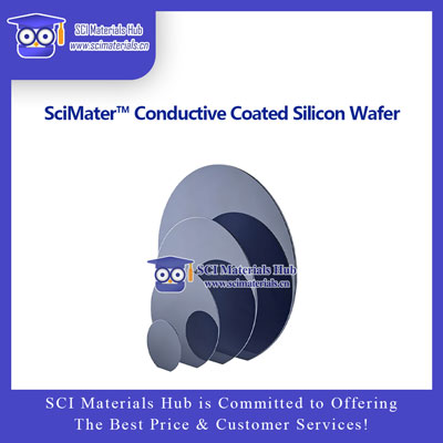
SciMater™ Conductive Coated Silicon Wafer

  • Product Code:
  • Description:SciMater™ Conductive Coated Silicon Wafer
  • Brand:SciMater™
  • Lead time:Please ask
  • Views:
  • Telephone:+86 153-5789-9751; +86 156-0553-2352
  • Keywords:SciMater™ Conductive Coated Silicon Wafer, SCI Materials Hub
METAL-COATED SILICON SUBSTRATES

SciMater™ Metal-Coated Conductive Silicon Wafers

Monocrystalline silicon wafers coated with functional Au, Pt, Ag, Cu, and other films for use as conductive electrodes, thin-film substrates, microelectronic device platforms, and materials-testing surfaces. Full 2-inch, 4-inch, and 6-inch wafers and multiple small cut-piece sizes are available, together with extended aluminum-coated and Si₃N₄-coated options.

Au-Coated Silicon Pt-Coated Silicon Ag-Coated Silicon Cu-Coated Silicon Full Wafers / Cut Pieces

Product Overview

Metal-coated silicon wafers combine a monocrystalline silicon substrate with a functional surface film. They can be used for conductive contacts, electrode fabrication, sensors, micro-/nanofabrication, thin-film deposition, and optoelectronic testing. Each metal offers different conductivity, chemical stability, surface reactivity, and process compatibility, so selection should be based on the experimental environment, contact method, and device structure.

The nominal Au thickness for full wafers and Au cut pieces is 100 nm. The nominal thickness is 150 nm for the 4-inch Pt-coated wafer and 300 nm for the 4-inch Al-coated wafer. Film thicknesses for Pt, Ag, and Cu cut pieces, as well as Ti/Cr adhesion layers, were not specified in the original data and must be confirmed by batch or order. Si₃N₄ is an insulating dielectric film rather than a conductive metal film.
Multiple Film Materials

Available with Au, Pt, Ag, Cu, Al, Si₃N₄, and other functional films.

Full Wafers and Cut Pieces

Available as full 2–6 inch wafers and common cut-piece sizes from 5 mm to 20 mm.

Broad Experimental Compatibility

Suitable for electrodes, sensors, thin-film deposition, optoelectronic, and microelectronic research.

Configurable Specifications

Substrate, film thickness, adhesion layer, polishing, and packaging can be confirmed as required.

Film Material Characteristics

Au
Gold-Coated Silicon Wafer

Offers good surface stability for electrodes, sensing, surface modification, microelectronics, and optical experiments.

Pt
Platinum-Coated Silicon Wafer

Provides good chemical resistance and thermal stability for electrochemical electrodes, catalysis, and high-temperature contact studies.

Ag
Silver-Coated Silicon Wafer

Combines strong electrical conductivity with optical response for electrodes, optics, and surface-enhanced studies.

Cu
Copper-Coated Silicon Wafer

Suitable for conductive interconnects, electrodes, and metal-film research; surface oxidation must be controlled during use and storage.

Al
Aluminum-Coated Silicon Wafer

Suitable for electrodes, reflective films, microelectronics, and metal-film processing; a native oxide layer may form on the surface.

Si₃N₄
Silicon Nitride-Coated Wafer

An insulating dielectric film suitable for passivation, isolation, masking, MEMS, and micro-/nanofabrication.

Complete Product Specifications

Products with duplicate names and identical specifications have been consolidated. All full wafers and cut pieces are shown in one comparison table.

Product CategoryFinished SizeSubstrate / PolishingFilm MaterialNominal Film ThicknessSurface or OrientationPrimary Use
Full Metal-Coated Wafer2 InchSilicon substrate; polishing to be confirmedAu100 nmConfirm by BatchConductive electrodes, thin films, and device experiments
Full Dielectric-Coated Wafer4 InchSilicon substrate; polishing to be confirmedSi₃N₄Not SpecifiedInsulating Silicon Nitride FilmPassivation, isolation, masking, and MEMS
Full Metal-Coated Wafer4 InchSilicon substrate; polishing to be confirmedAu100 nmConfirm by BatchConductive electrodes, sensing, and optoelectronic experiments
Full Metal-Coated Wafer4 InchSilicon substrate; polishing to be confirmedPt150 nmPt (111) Orientation DescriptionConductive, electrochemical, and microelectronic testing
Full Metal-Coated Wafer4 InchSilicon substrate; polishing to be confirmedAl300 nmConfirm by BatchElectrodes, reflective films, and microelectronic processing
Full Metal-Coated Wafer6 InchSilicon substrate; polishing to be confirmedAu100 nmConfirm by BatchLarge-area conductive and device processing
Gold-Coated Cut Piece5 × 5 mmSingle-Side Polished SiliconAu100 nmSingle-Side CoatedSmall-area electrode and materials experiments
Gold-Coated Cut Piece8 × 8 mmSingle-Side Polished SiliconAu100 nmSingle-Side CoatedSensing, coating, and conductivity experiments
Gold-Coated Cut Piece10 × 10 mmSingle-Side Polished SiliconAu100 nmSingle-Side CoatedCommon electrode and microdevice substrate
Gold-Coated Cut Piece15 × 15 mmSingle-Side Polished SiliconAu100 nmSingle-Side CoatedMedium-area conductive and optoelectronic experiments
Gold-Coated Cut Piece20 × 20 mmSingle-Side Polished SiliconAu100 nmSingle-Side CoatedLarger-area electrode and device processing
Platinum-Coated Cut Piece10 × 10 mmSilicon substrate; polishing to be confirmedPtNot SpecifiedConfirm by BatchElectrochemistry, catalysis, and electrode testing
Copper-Coated Cut Piece5 × 5 mmSilicon substrate; polishing to be confirmedCuNot SpecifiedConfirm by BatchConductive interconnect and metal-film experiments
Copper-Coated Cut Piece8 × 8 mmSilicon substrate; polishing to be confirmedCuNot SpecifiedConfirm by BatchConductive interconnect and metal-film experiments
Copper-Coated Cut Piece10 × 10 mmSilicon substrate; polishing to be confirmedCuNot SpecifiedConfirm by BatchElectrode, interconnect, and device research
Copper-Coated Cut Piece15 × 15 mmSilicon substrate; polishing to be confirmedCuNot SpecifiedConfirm by BatchMedium-area conductive-film experiments
Copper-Coated Cut Piece20 × 20 mmSilicon substrate; polishing to be confirmedCuNot SpecifiedConfirm by BatchLarger-area conductive-film experiments
Silver-Coated Cut Piece5 × 5 mmSilicon substrate; polishing to be confirmedAgNot SpecifiedConfirm by BatchConductivity, optics, and surface experiments
Silver-Coated Cut Piece10 × 10 mmSilicon substrate; polishing to be confirmedAgNot SpecifiedConfirm by BatchElectrode, optical, and sensing research
Silver-Coated Cut Piece15 × 15 mmSilicon substrate; polishing to be confirmedAgNot SpecifiedConfirm by BatchMedium-area conductive and optical experiments
Silver-Coated Cut Piece20 × 20 mmSilicon substrate; polishing to be confirmedAgNot SpecifiedConfirm by BatchLarger-area electrode and optical experiments
Any listed prices correspond to standard reference configurations. Silicon size and thickness, conductivity type, crystal orientation, polishing, film thickness, thickness tolerance, adhesion layer, surface roughness, patterning, inspection documentation, and packaging may affect the final quotation.

Main Applications

Conductive Electrodes

For planar electrodes, contact electrodes, backside electrodes, and electrical test structures.

Electrochemistry and Catalysis

Au and Pt films can be used for electrochemical electrodes, catalysis, and interfacial-reaction research.

Sensors

Suitable for gas, biological, chemical, optoelectronic, and microsensor development.

Microelectronic Devices

For metal contacts, conductive interconnects, test structures, and micro-/nanodevice fabrication.

Optoelectronics and Optics

Suitable for reflective films, optical electrodes, surface enhancement, and photoelectric-conversion experiments.

Thin-Film and Materials Research

Can serve as a supporting substrate for two-dimensional materials, oxides, polymers, and other functional materials.

Surface Modification

Metal surfaces can support molecular immobilization, interface functionalization, and biosensing research.

MEMS and Micro-/Nanofabrication

Suitable for microelectrodes, microheaters, microstructures, and patterned-metal processing.

Materials Characterization

For SEM, AFM, Raman, contact-angle, resistance, and film-performance measurements.

Selection Guide

General Conductive Electrodes
Au-coated silicon is a common first choice. Confirm film thickness, adhesion layer, and electrical-contact method before use.
Electrochemical and Catalytic Experiments
Choose Pt- or Au-coated silicon and verify compatibility with the electrolyte, working potential, and cleaning procedure.
Cost-Sensitive Conductivity Experiments
Cu-coated silicon can be selected, but air exposure should be minimized and surface oxidation controlled.
Optical and Surface-Enhanced Applications
Choose Ag or Au according to the target wavelength and experimental design, and confirm surface-roughness requirements.
Reflective Films and Electrodes
Al-coated silicon may be used, with consideration of the native surface oxide layer.
Insulation and Passivation Layers
Choose Si₃N₄-coated silicon; it should not be treated as a conventional conductive metal film.
Small-Area Experiments
Choose 5 × 5 mm, 8 × 8 mm, or 10 × 10 mm cut pieces.
Larger-Area Processing
Choose 15 × 15 mm or 20 × 20 mm cut pieces, or full 2–6 inch wafers.

How to Use

1
Verify Product Parameters

Confirm size, film material, film thickness, coated side, substrate, and package label.

2
Clean Handling

Wear powder-free gloves and handle the edge using a vacuum wand or flat-tip tweezers.

3
Identify the Coated Side

Use the package identification; do not scratch the surface or use friction to identify the film.

4
Gentle Cleaning

Remove loose particles with clean nitrogen. Ordinary tissues should not be used directly on the surface.

5
Mounting and Fixturing

Use a compatible fixture and prevent clamp marks in the active metal-film area.

6
Establish Electrical Contact

Use probes, conductive adhesive, spring contacts, or patterned electrodes according to the experiment.

7
Perform Downstream Processing

Proceed with photolithography, etching, deposition, surface modification, or device testing as required.

8
Sealed Storage

After use, clean as appropriate and reseal the substrate in a clean carrier or package.

Handling, Cleaning, and Storage

Prevent Film Scratches

Do not rub the metal surface with sharp tweezers, ordinary tissues, or rough materials.

Prevent Fingerprint Contamination

Fingerprints and oils can affect electrical contact, surface modification, and subsequent coating.

Select Cleaning Agents Carefully

Chemical resistance varies by metal; confirm compatibility between the cleaning agent and the film before use.

Control Cu Surface Oxidation

Use Cu-coated silicon promptly after opening and keep it dry and sealed.

Protect Ag from Tarnishing

Keep silver-coated surfaces away from sulfur-containing environments and corrosive gases to reduce tarnishing and contamination.

Confirm High-Temperature Compatibility

High-temperature treatment may cause diffusion, oxidation, stress changes, or reduced film adhesion.

FAQ

1. What are the differences between Au-, Pt-, Ag-, and Cu-coated silicon wafers?

The metals differ in chemical stability, conductivity, surface activity, optical behavior, and process compatibility. Au is suitable for general electrodes and surface modification, Pt for electrochemistry and catalysis, Ag for conductivity and optical studies, and Cu for interconnects and cost-sensitive conductivity experiments.

2. Is there a Ti or Cr adhesion layer beneath the metal film?

The original specifications do not consistently identify an adhesion layer. Au, Pt, and other metals may require a Ti or Cr transition layer on silicon or SiO₂. Confirm the complete layer structure before ordering when it is important.

3. What is the film thickness of the Au-coated cut pieces?

The current 5 × 5 mm to 20 × 20 mm single-side polished Au-coated cut pieces are listed with a nominal Au thickness of 100 nm. Thickness tolerance and adhesion-layer details are subject to the corresponding batch or confirmed order.

4. What are the film thicknesses of the Pt-, Ag-, and Cu-coated cut pieces?

The source specifications do not state the exact film thicknesses for these cut pieces. Film thickness, tolerance, adhesion layer, and deposition method must be confirmed before purchase and should not be inferred from the full-wafer specifications.

5. What does 4-inch Pt (111) mean?

Pt (111) generally describes a crystallographic orientation characteristic of the platinum film. The degree of orientation, measurement method, and peak intensity are subject to the corresponding XRD or batch inspection data.

6. Can a metal-coated silicon wafer be used directly as an electrode?

It can be used as a conductive electrode or test substrate, but performance also depends on film thickness, film continuity, adhesion layer, surface contamination, contact method, and operating environment.

7. Can the metal surface undergo additional photolithography or coating?

Yes. Photolithography, patterning, secondary deposition, and surface modification are possible, but the effects of photoresist, developer, etchant, plasma treatment, and temperature on the existing metal film must be evaluated first.

8. How should Cu- and Ag-coated silicon wafers be stored?

Store them in a clean, dry, sealed environment with minimal exposure to air, high humidity, sulfur-containing gases, and corrosive gases. Use promptly after opening and reseal unused pieces.

9. Is a Si₃N₄-coated silicon wafer conductive?

Si₃N₄ is generally used as an insulating dielectric film, passivation layer, or etch mask and is not a conventional conductive film. For a conductive surface, choose a metal-coated wafer or fabricate separate electrodes.

10. Can the size, film thickness, and layer structure be customized?

Silicon-wafer size, cut dimensions, film material, film thickness, adhesion layer, single- or double-side coating, patterning, cleaning, inspection, and packaging can be evaluated according to project requirements.

Ordering Information

Recommended Inquiry Format

Full Wafer/Cut Piece + Size + Silicon Type and Polishing + Film Material + Film Thickness + Adhesion Layer + Single-/Double-Side Coating + Quantity + Inspection and Packaging Requirements.

Example: 10 × 10 mm + single-side polished silicon + Au 100 nm + confirm Ti/Cr adhesion layer + single-side coating + 20 pieces + individually packaged in clean carriers.

Product Summary

Au-, Pt-, Ag-, and Cu-coated silicon wafers can serve as conductive electrodes, thin-film substrates, and microelectronic-processing platforms for electrochemistry, sensors, optoelectronics, micro-/nanofabrication, and materials characterization. Au is suitable for general electrodes and surface modification, Pt for electrochemistry and catalysis, Ag for conductivity and optical research, and Cu for interconnect and metal-film experiments. Before purchasing, confirm substrate parameters, film thickness, adhesion layer, coated side, surface condition, and storage requirements, and use the confirmed order and batch documentation as the final acceptance basis.

Single-Side Polished Coated Silicon Wafer USD Price Table

Single-Side Polished Coated Silicon Wafer Price Table

Coating Type × Size × Conductivity Type × Crystal Orientation Price Matrix

Covers Au-, Cu-, Ag-, Pt-, Si₃N₄-, and Al-coated silicon wafers, allowing quick price selection by size, N-type or P-type conductivity, and crystal orientation.

Price
Substrate:Single-Side Polished Silicon Wafer
Conductivity Type:N-Type / P-Type
Crystal Orientation:100 / 110 / 111
Coating:Au / Cu / Ag / Pt / Si₃N₄ / Al
Price Unit:USD / Wafer
Coating SystemSizeCoating SpecificationN-Type SSP SiliconP-Type SSP Silicon
Orientation 100Orientation 110Orientation 111Orientation 100Orientation 110Orientation 111
Au-Coated SSP Au-Coated Silicon Covers small cut pieces and 2-, 4-, and 6-inch wafers.5 × 5 mmAu 100 nm $8$8$8$8$8$8
8 × 8 mm$10$10$10$10$10$10
10 × 10 mm$14$14$14$14$14$14
15 × 15 mm$34$34$34$34$34$34
20 × 20 mm$57$57$57$57$57$57
2 Inch$152$152$152$152$152$152
4 Inch$286$286$286$286$286$286
6 Inch$560$560$560$560$560$560
Cu-Coated SSP Cu-Coated Silicon Available in square cut pieces from 5 × 5 mm to 20 × 20 mm.5 × 5 mmCu Coating$6$6$6$6$6$6
8 × 8 mmCu Coating$8$8$8$8$8$8
10 × 10 mmCu Coating$9$9$9$9$9$9
15 × 15 mmCu Coating$12$12$12$12$12$12
20 × 20 mmCu Coating$14$14$14$14$14$14
Ag-Coated SSP Ag-Coated Silicon Available in multiple small Ag-coated silicon sizes.5 × 5 mmAg Coating$6$6$6$6$6$6
10 × 10 mmAg Coating$10$10$10$10$10$10
15 × 15 mmAg Coating$14$14$14$14$14$14
20 × 20 mmAg Coating$18$18$18$18$18$18
Pt-Coated SSP Pt-Coated Silicon Includes a small cut piece and a 4-inch Pt 150 nm wafer.10 × 10 mmPt Coating$22$22$22$22$22$22
4 InchPt 150 nm $384$384$384$384$384$384
Silicon Nitride Film Si₃N₄-Coated Silicon 4-inch single-side polished silicon nitride-coated wafer.4 InchSi₃N₄ Film$107$107$107$107$107$107
Al-Coated SSP Al-Coated Silicon 4-inch Al 300 nm single-side polished silicon wafer.4 InchAl 300 nm $221$221$221$221$221$221
Email for Quotationscontact@scimaterials.cn
WhatsApp & Telephone+86 153-7569-8751
International Sales ChannelseBay, Amazon, and Alibaba stores are available for quick ordering.
Worldwide ShippingDHL, FedEx, UPS, SF Express, or another requested carrier.
Bulk OrdersVolume discounts are available upon request.
Accepted PaymentsBank wire transfer, PayPal, credit card, Alipay, and WeChat Pay.

Partial references citing our materials (from Google Scholar)


Carbon Dioxide Reduction

1. ACS Nano Strain Relaxation in Metal Alloy Catalysts Steers the Product Selectivity of Electrocatalytic CO2 Reduction

The bipolar membrane (Fumasep FBM) in this paper was purchased from SCI Materials Hub, which was used in rechargeable Zn-CO2 battery tests. The authors reported a strain relaxation strategy to determine lattice strains in bimetal MNi alloys (M = Pd, Ag, and Au) and realized an outstanding CO2-to-CO Faradaic efficiency of 96.6% with outstanding activity and durability toward a Zn-CO2 battery.


2. Front. Chem. Boosting Electrochemical Carbon Dioxide Reduction on Atomically Dispersed Nickel Catalyst

In this paper, Vulcan XC-72R was purchased from SCI Materials Hub. Vulcan XC 72R carbon is the most common catalyst support used in the anode and cathode electrodes of Polymer Electrolyte Membrane Fuel Cells (PEMFC), Direct Methanol Fuel Cells (DMFC), Alkaline Fuel Cells (AFC), Microbial Fuel Cells (MFC), Phosphoric Acid Fuel Cells (PAFC), and many more!


3. Adv. Mater. Partially Nitrided Ni Nanoclusters Achieve Energy-Efficient Electrocatalytic CO2 Reduction to CO at Ultralow Overpotential

An AEM membrane (Sustainion X37-50 Grade RT, purchased from SCI Materials Hub) was activated in 1 M KOH for 24 h, washed with ultra-purity water prior to use.


4. Adv. Funct. Mater. Nanoconfined Molecular Catalysts in Integrated Gas Diffusion Electrodes for High-Current-Density CO2 Electroreduction

In this paper (Supporting Information), an anion exchanged membrane (Fumasep FAB-PK-130 obtained from SCI Materials Hub (www.scimaterials.cn)) was used to separate the catholyte and anolyte chambers.

SCI Materials Hub: we also recommend our Fumasep FAB-PK-75 for the use in a flow cell.


5. Appl. Catal. B Efficient utilization of nickel single atoms for CO2 electroreduction by constructing 3D interconnected nitrogen-doped carbon tube network

In this paper, the Nafion 117 membrane was obtained from SCI Materials Hub.


6. Vacuum Modulable Cu(0)/Cu(I)/Cu(II) sites of Cu/C catalysts derived from MOF for highly selective CO2 electroreduction to hydrocarbons

In this paper, Proton exchange membrane (Nafion 117), Nafion D520, and Toray 060 carbon paper were purchased from SCI Materials Hub.


7. National Science Review Confinement of ionomer for electrocatalytic CO2 reduction reaction via efficient mass transfer pathways

An anion exchange membrane (PiperION-A15-HCO3) was obtained from SCI Materials Hub.


8. Catalysis Communications Facilitating CO2 electroreduction to C2H4 through facile regulating {100} & {111} grain boundary of Cu2O

Carbon paper (TGPH060), membrane solution (Nafion D520), and ionic membrane (Nafion N117) were obtained from Wuhu Eryi Material Technology Co., Ltd (a company under SCI Materials Hub).


Batteries

1. J. Mater. Chem. A Blocking polysulfides with a Janus Fe3C/N-CNF@RGO electrode via physiochemical confinement and catalytic conversion for high-performance lithium–sulfur batteries

Graphene oxide (GO) in this paper was obtained from SCI Materials Hub. The authors introduced a Janus Fe3C/N-CNF@RGO electrode consisting of 1D Fe3C decorated N-doped carbon nanofibers (Fe3C/N-CNFs) side and 2D reduced graphene oxide (RGO) side as the free-standing carrier of Li2S6 catholyte to improve the overall electrochemical performance of Li-S batteries.


2. Joule A high-voltage and stable zinc-air battery enabled by dual-hydrophobic-induced proton shuttle shielding

This paper used more than 10 kinds of materials from SCI Materials Hub and the authors gave detailed properity comparsion.

The commercial IEMs of Fumasep FAB-PK-130 and Nafion N117 were obtained from SCI Materials Hub.

Gas diffusion layers of GDL340 (CeTech) and SGL39BC (Sigracet) and Nafion dispersion (Nafion D520) were obtained from SCI Materials Hub.

Zn foil (100 mm thickness) and Zn powder were obtained from the SCI Materials Hub.

Commercial 20% Pt/C, 40% Pt/C and IrO2 catalysts were also obtained from SCI Materials Hub.


3. Journal of Energy Chemistry Vanadium oxide nanospheres encapsulated in N-doped carbon nanofibers with morphology and defect dual-engineering toward advanced aqueous zinc-ion batteries

In this paper, carbon cloth (W0S1011) was obtained from SCI Materials Hub. The flexible carbon cloth matrix guaranteed the stabilization of the electrode and improved the conductivity of the cathode.


4. Energy Storage Materials Defect-abundant commercializable 3D carbon papers for fabricating composite Li anode with high loading and long life

The 3D carbon paper (TGPH060 raw paper) were purchased from SCI Materials Hub.


5. Nanomaterials A Stable Rechargeable Aqueous Zn–Air Battery Enabled by Heterogeneous MoS2 Cathode Catalysts

Nafion D520 (5 wt%), and carbon paper (GDL340) were received from SCI-Materials-Hub.


6. SSRN An Axially Directed Cobalt-Phthalocyanine Covalent Organic Polymer as High-Efficient Bifunctional Catalyst for Zn-Air Battery

Carbon cloth (W0S1011) and other electrochemical consumables required for air cathode were provided by SCI Materials Hub.


Oxygen Reduction Reaction

1. J. Chem. Eng. Superior Efficiency Hydrogen Peroxide Production in Acidic Media through Epoxy Group Adjacent to Co-O/C Active Centers on Carbon Black

In this paper, Vulcan XC 72 carbon black, ion membrane (Nafion N115, 127 μL), Nafion solution (D520, 5 wt%), and carbon paper (AvCarb GDS 2230 and Spectracarb 2050A-1050) were purchased from SCI Materials Hub.


2. Journal of Colloid and Interface Science Gaining insight into the impact of electronic property and interface electrostatic field on ORR kinetics in alloy engineering via theoretical prognostication and experimental validation

The 20 wt% Pt3M (M = Cr, Co, Cu, Pd, Sn, and Ir) were purchased from SCI Materials Hub. This work places emphasis on the kinetics of the ORR concerning Pt3M (M = Cr, Co, Cu, Pd, Sn, and Ir) catalysts, and integrates theoretical prognostication and experimental validation to illuminate the fundamental principles of alloy engineering.


Water Electrolysis

1. International Journal of Hydrogen Energy Gold as an efficient hydrogen isotope separation catalyst in proton exchange membrane water electrolysis

The cathodic catalysts of Pt/C (20 wt%, 2–3 nm) and Au/C (20 wt%, 4–5 nm) were purchased from SCI Materials Hub.


2. Small Science Silver Compositing Boosts Water Electrolysis Activity and Durability of RuO2 in a Proton-Exchange-Membrane Water Electrolyzer

Two fiber felts (0.35 mm thickness, SCI Materials Hub) were used as the porous transport layers at both the cathode and the anode.


3. Advanced Functional Materials Hierarchical Crystalline/Amorphous Heterostructure MoNi/NiMoOx for Electrochemical Hydrogen Evolution with Industry-Level Activity and Stability

Anion-exchange membrane (FAA-3-PK-130) was obtained from SCI Materials Hub website.


Fuel Cells

1. Polymer Sub-two-micron ultrathin proton exchange membrane with reinforced mechanical strength

Gas diffusion electrode (60% Pt/C, Carbon paper) was purchased from SCI Materials Hub.


Characterization

1. Chemical Engineering Journal Electrochemical reconstitution of Prussian blue analogue for coupling furfural electro-oxidation with photo-assisted hydrogen evolution reaction

An Au nanoparticle film was deposited on the total reflecting plane of a single reflection ATR crystal (SCI Materials Hub, Wuhu, China) via sputter coater.


Related Products

We Provide A Broad Range of Materials, Instruments & Solutions in Advanced Science and Technologies About Us
Product consultation
Customer service1
Customer service2
After-sales and technical consultation
Customer service1
Customer service2
WeChat Customer Service

Back to top