Welcome to the SCI Materials Hub !
Home > Silicon Wafer > Other > SciMater™ Monocrystalline Silicon Double-Side Lapped Wafers

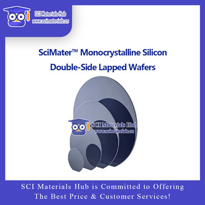
SciMater™ Monocrystalline Silicon Double-Side Lapped Wafers

  • Product Code:
  • Description:SciMater™ Monocrystalline Silicon Double-Side Lapped Wafers
  • Brand:SciMater™
  • Lead time:Please ask
  • Views:
  • Telephone:+86 153-5789-9751; +86 156-0553-2352
  • Keywords:SciMater™ Monocrystalline Silicon Double-Side Lapped Wafers, SCI Materials Hub
SciMater™ Semiconductor Substrates

SciMater™ Single-Side / Double-Side Polished Monocrystalline Silicon Wafers

High-purity monocrystalline silicon substrates for integrated circuits, microelectronic devices, MEMS, sensors, optoelectronics, thin-film deposition, micro- and nanofabrication, and university research.

SSP: Single-Side Polished DSP: Double-Side Polished 1–8 Inch Options N-Type / P-Type / Intrinsic <100>/<111> Custom Cutting & Coating

Product Overview

SciMater™ Single-Side and Double-Side Polished Monocrystalline Silicon Wafers are manufactured from high-purity single-crystal silicon through slicing, edge rounding, lapping, cleaning, and chemical-mechanical polishing. They are suitable for semiconductor devices, thin-film materials, photolithography, etching, MEMS, sensors, and micro-/nanostructure fabrication.

A single-side polished wafer, abbreviated SSP, has one precision-polished surface. Its back surface is generally lapped, etched, or otherwise process-finished. SSP wafers are suitable for most single-sided lithography, coating, etching, and material-growth experiments.

A double-side polished wafer, abbreviated DSP, has both front and back surfaces precision polished. DSP wafers are recommended for double-sided processing, transmission measurements, wafer bonding, deep silicon etching, microfluidics, and applications requiring improved overall flatness.

Standard wafer sizes from 1 to 8 inches are available. N-type, P-type, intrinsic undoped,<100>,<111>, multiple resistivity ranges, thicknesses, and orientation features can be confirmed according to project requirements. Final specifications are subject to the batch label, inspection documentation, or confirmed order.

Key Features

High-Purity Monocrystalline SiliconUniform crystal structure for semiconductor processing, device fabrication, and materials research.
Precision-Polished SurfaceFlat and smooth process surfaces for photolithography, deposition, etching, epitaxy, and surface modification.
SSP and DSP OptionsSSP balances performance and cost; DSP supports double-sided processing and high-flatness applications.
Multiple Crystal OrientationsCommon options include<100>and<111>; other orientations may be evaluated.
Multiple Conductivity TypesN-type, P-type, intrinsic undoped, low-resistivity, and high-resistivity silicon options.
Wide Size CoverageAvailable in 1-, 2-, 3-, 4-, 5-, 6-, and 8-inch wafer formats.
Special ThicknessesStandard, ultra-thin, extra-thick, and customized thickness options can be assessed.
Downstream ProcessingCustom cutting, oxidation, nitridation, metal coating, drilling, and special-shape processing.

Single-Side vs. Double-Side Polished Wafers

Comparison ItemSingle-Side Polished WaferDouble-Side Polished Wafer
AbbreviationSSP, Single-Side PolishedDSP, Double-Side Polished
Polished SurfacesOne precision-polished surfaceBoth front and back surfaces precision polished
Back-Surface ConditionLapped, etched, or process-finishedPrecision-polished surface
Relative CostLowerHigher
Main AdvantageCost-effective for most routine microfabrication and thin-film experimentsBoth surfaces are flat and smooth for double-sided processing, bonding, and transmission measurements
Typical ApplicationsLithography, coating, etching, material growth, and routine device fabricationWafer bonding, double-sided lithography, deep silicon etching, MEMS, and optical testing
Equipment UseCompatible with most standard wafer equipment and vacuum chucksThe back polished surface must be protected from chuck marks and particle scratches
Recommended ForGeneral research, material deposition, and single-sided device processingDouble-sided processing, transmission, bonding, or high-flatness applications

Standard Sizes and Reference Prices

Wafer SizeNominal DiameterSSP Reference Price (CNY / Wafer)DSP Reference Price (CNY / Wafer)
1 InchØ25.4 mmCNY 30CNY 40
2 InchØ50.8 mmCNY 40CNY 50
3 InchØ76.2 mmCNY 60CNY 70
4 InchØ100 mmCNY 80CNY 90
5 InchØ125 mmCNY 85CNY 90
6 InchØ150 mmCNY 90CNY 95
8 InchØ200 mmCNY 105CNY 150
Prices shown are references for standard base specifications. Final pricing may vary with crystal orientation, conductivity type, resistivity, thickness, flatness, surface quality, packaging, and inspection requirements.

Technical Parameters

ParameterStandard Options
MaterialHigh-purity monocrystalline silicon
PolishingSingle-side polished or double-side polished
Wafer Size1, 2, 3, 4, 5, 6, and 8 inches
Conductivity TypeN-type, P-type, or intrinsic undoped
Common DopantsPhosphorus for N-type and boron for P-type
Crystal Orientation<100>and<111>; other orientations may be available
ResistivityLow, standard, high, or customized resistivity ranges
ThicknessStandard, ultra-thin, extra-thick, or customized thickness
Surface ConditionBare polished silicon; optional SiO₂, Si₃N₄, or metal coatings
Orientation FeaturePrimary flat, primary/secondary flats, notch, or size-dependent standard
Flatness ParametersThickness tolerance, TTV, Bow, and Warp may be specified
Cutting ServicesSquare, rectangular, circular, mechanical dicing, laser cutting, drilling, and special shapes
PackagingSingle-wafer box, multi-wafer box, vacuum packaging, clean bag, or customized packaging

Important Selection Parameters

ParameterMeaning and Selection Guidance
Conductivity TypeElectrons are the primary carriers in N-type silicon, while holes are the primary carriers in P-type silicon. Select according to the device architecture and test plan.
Crystal Orientation<100>is widely used in integrated circuits, MOS, and MEMS;<111>is often used for epitaxy, surface studies, and selected orientation-dependent etching.
ResistivityLow resistivity supports conductive substrates; high resistivity supports low-leakage, RF, microwave, and insulation-related experiments.
ThicknessStandard thickness is easy to handle; ultra-thin wafers support special devices; thick wafers improve mechanical support and deep processing.
TTVTotal Thickness Variation describes thickness uniformity across different wafer locations.
BowThe center displacement of a free, unclamped wafer relative to a reference plane.
WarpThe overall difference between the wafer's highest and lowest points.
Surface RoughnessSmoother surfaces are better suited for fine lithography, ultrathin-film deposition, bonding, and micro-/nanodevice fabrication.

Main Applications

1. Semiconductor Devices and Integrated CircuitsDiodes, transistors, MOS devices, capacitors, test electrodes, and microelectronic device research.
2. Photolithography and Micro-/NanofabricationSpin coating, exposure, development, electron-beam lithography, nanoimprint, etching, and pattern transfer.
3. Thin-Film Deposition and Material GrowthMagnetron sputtering, thermal evaporation, e-beam evaporation, CVD, ALD, MBE, and spin coating.
4. MEMS and SensorsPressure sensors, accelerometers, microheaters, microelectrodes, and inertial-device fabrication.
5. Optoelectronics and Micro-/Nano-OpticsPhotodetectors, solar cells, gratings, reflective structures, filters, and photonic devices.
6. Wafer Bonding and MicrofluidicsDSP wafers support silicon-to-silicon bonding, silicon-to-glass bonding, microchannels, and microreactors.
7. Materials CharacterizationSubstrates for Raman, XRD, SEM, AFM, ellipsometry, film-thickness, contact-angle, and Hall measurements.
8. Teaching and Equipment QualificationSemiconductor-process education and process validation for lithography, coating, and etching equipment.

Selection Guide

Choosing SSP or DSP

Application RequirementRecommended Product
Front-side lithography, coating, or etching onlySingle-side polished wafer
General material growth or thin-film characterizationSingle-side polished wafer
Lower experimental costSingle-side polished wafer
Processing required on both surfacesDouble-side polished wafer
Wafer bondingDouble-side polished wafer
Double-sided lithography or deep silicon etchingDouble-side polished wafer
Transmission optical measurementsDouble-side polished wafer
MEMS membrane structures or microchannelsDouble-side polished wafer preferred

Choosing Wafer Size

Application ScenarioRecommended Size
Small-area materials tests, teaching, and low-volume sample preparation1-inch, 2-inch, or cut pieces
Routine laboratory lithography, coating, and device fabrication2-inch or 3-inch
University micro-/nanofabrication platforms and semiconductor processing4-inch
Larger-area films, pilot processing, and device arrays5-inch or 6-inch
Large-area semiconductor processes and industrial equipment8-inch
Small-area testing only5 mm × 5 mm, 10 mm × 10 mm, or 20 mm × 20 mm cut pieces

How to Use

1Incoming InspectionVerify size, polishing, conductivity type, orientation, resistivity, thickness, quantity, and packaging condition.
2Clean HandlingWear powder-free gloves or finger cots and handle wafer edges with a vacuum wand or wafer tweezers.
3Identify the Polished SurfaceThe polished face of an SSP wafer generally produces a clearer reflection. Both DSP surfaces must be protected.
4Surface CleaningSelect compatible solvents, deionized water, plasma treatment, or standard wafer-cleaning procedures.
5PhotolithographyAfter dehydration, center the wafer on the spin coater and confirm stable vacuum holding before coating, exposure, and development.
6Coating and DepositionConfirm equipment and fixture compatibility, and validate surface activation or pretreatment on a small sample when needed.
7Dicing and CuttingDiamond scribing, dicing saws, or laser cutting may be used while protecting the polished surface.
8Double-Sided ProcessingUse suitable carriers and fixtures for DSP wafers to prevent back-surface scratches, particles, and chuck marks.

Cleaning, Storage, and Maintenance

Cleaning Guidance

Cleaning ItemRecommendation
Organic ContaminationUse a process-compatible organic solvent and prevent solvent residue.
Particle ContaminationUse deionized-water rinsing, ultrasonic, or megasonic cleaning; use ultrasonic cleaning cautiously with ultra-thin wafers.
Native OxideBare silicon naturally develops an oxide layer in air. Sensitive interface experiments require planned surface treatment.
Metal ContaminationUse clean vessels and high-purity reagents to reduce adverse effects on semiconductor-device performance.
Ultra-Thin WafersReduce mechanical stress during cleaning, drying, and handling to prevent breakage and warpage.
DSP WafersBoth surfaces are functional surfaces; do not place them directly on rough benches or ordinary paper.

Storage Guidance

Storage ItemRecommendation
EnvironmentClean, dry, and protected from light; keep away from acidic, alkaline, and corrosive vapors.
PackagingKeep unused wafers in the original wafer box, clean bag, or vacuum packaging.
Surface ProtectionPrevent polished surfaces from contacting hard objects, paper fibers, plastic debris, or other wafers.
Opened PackagesUse promptly after opening; reseal remaining wafers and record the batch and opening date.
Long-Term StorageUse a clean, dry cabinet and control humidity and particle contamination.
DSP WafersUse spaced or non-contact packaging to prevent the two polished surfaces from rubbing.

Ordering Information

Please provide the following information when requesting a quotation:

Size + SSP / DSP + Conductivity Type + Crystal Orientation + Resistivity + Thickness + Quantity + Orientation Feature + Packaging

Standard example: 4 inch + double-side polished + P-type +<100>+ 1–10 Ω·cm + 525 μm thickness + 25 wafers + individually packed.

For custom cutting: target dimensions + thickness + quantity + dimensional tolerance + cutting method + cleaning + packaging.

For custom coating: coating material + coating thickness + single-/double-side coating + adhesion-layer requirement + quantity.

FAQ

1. What is the main difference between SSP and DSP wafers?

An SSP wafer has one primary precision process surface and is less expensive, making it suitable for routine lithography, coating, and etching. A DSP wafer has two polished surfaces and is recommended for double-sided processing, bonding, transmission measurements, and high-precision MEMS.

2. Is a DSP wafer always higher quality than an SSP wafer?

Not necessarily. DSP only indicates that both surfaces are precision polished. It does not mean that every electrical or geometric parameter is automatically superior. Select DSP when the back surface must function as a process surface.

3. How should I choose between N-type and P-type?

Choose according to the device architecture, carrier type, and electrical test plan. For general deposition or morphology studies, conductivity type may be less critical, so cost and available stock may be prioritized.

4. What is the difference between<100>and<111>orientations?

<100>is commonly used for MOS devices, integrated circuits, and MEMS.<111>is often used in selected epitaxy, surface science, orientation-dependent etching, and specialized device research.

5. Are the wafers supplied with an oxide layer by default?

Standard wafers are generally supplied as bare polished silicon, although a thin native oxide forms naturally in air. A specified thermal SiO₂ layer requires a separate oxidized-wafer product or custom oxidation process.

6. Are intrinsic, low-resistivity, and high-resistivity wafers available?

Availability depends on wafer size and batch. Intrinsic undoped wafers support low-carrier-background experiments, low-resistivity wafers support conductive substrates, and high-resistivity wafers support RF, microwave, low-leakage, and insulation-related research.

7. Can ultra-thin, extra-thick, or small custom-cut wafers be supplied?

These options can be evaluated according to dimensions, thickness, tolerance, and quantity. Ultra-thin wafers are fragile, while extra-thick wafers require verification of fixture and vacuum-chuck compatibility.

8. Can the wafer be used directly for photolithography?

Cleaning, dehydration, and surface preparation are recommended before use. High-precision lithography that is sensitive to particles, organics, or metal contamination should not use unverified wafers directly.

9. Can custom films be deposited on the wafer?

SiO₂, Si₃N₄, Au, Pt, Ag, Cu, Al, and other coatings can be evaluated. Adhesion layers, film thickness, single-/double-side coating, and patterning requirements should be confirmed with the order.

10. Why do wafers of the same diameter have different prices?

Pricing also depends on grade, SSP or DSP processing, conductivity type, orientation, resistivity, thickness, TTV, Bow, Warp, surface quality, inspection requirements, cutting, and packaging quantity.

Product Summary

Single-side polished monocrystalline silicon wafers offer moderate cost, convenient handling, and broad process compatibility for most front-side lithography, deposition, etching, material growth, and routine device fabrication. Double-side polished wafers provide functional polished surfaces on both sides for double-sided lithography, wafer bonding, deep silicon etching, transmission measurements, microfluidics, and precision MEMS. In addition to wafer diameter, confirm conductivity type, crystal orientation, resistivity, thickness, flatness, surface condition, and equipment compatibility before ordering.
Double-Side Ground Silicon Wafer USD Price Table

Double-Side Ground Silicon Wafer Price Table

Size × N/P Type × Crystal Orientation Price Matrix

Covers 2-inch to 6-inch double-side ground silicon wafers. Prices can be selected by wafer size, conductivity type, and crystal orientation 100, 110, or 111.

Product Type:Double-Side Ground Wafer
Conductivity Type:N-Type / P-Type
Crystal Orientation:100 / 110 / 111
Size:2–6 Inch
Price Unit:USD / Wafer
Product SeriesSizeSurface ConditionN-Type PriceP-Type Price
Orientation 100Orientation 110Orientation 111Orientation 100Orientation 110Orientation 111
Double-Side Ground Double-Side Ground · Unpolished Silicon Wafer Covers 2-inch to 6-inch wafers with N-type, P-type, and orientations 100, 110, and 111.
2 InchDouble-Side Ground$12$12$12$12$12$12
3 InchDouble-Side Ground$14$14$14$14$14$14
4 InchDouble-Side Ground$16$16$16$16$16$16
5 InchDouble-Side Ground$18$18$18$18$18$18
6 InchDouble-Side Ground$22$22$22$22$22$22
Email for Quotationscontact@scimaterials.cn
WhatsApp & Telephone+86 153-7569-8751
International Sales ChannelseBay, Amazon, and Alibaba stores are available for quick ordering.
Worldwide ShippingDHL, FedEx, UPS, SF Express, or another requested carrier.
Bulk OrdersVolume discounts are available upon request.
Accepted PaymentsBank wire transfer, PayPal, credit card, Alipay, and WeChat Pay.

Partial references citing our materials (from Google Scholar)


Carbon Dioxide Reduction

1. ACS Nano Strain Relaxation in Metal Alloy Catalysts Steers the Product Selectivity of Electrocatalytic CO2 Reduction

The bipolar membrane (Fumasep FBM) in this paper was purchased from SCI Materials Hub, which was used in rechargeable Zn-CO2 battery tests. The authors reported a strain relaxation strategy to determine lattice strains in bimetal MNi alloys (M = Pd, Ag, and Au) and realized an outstanding CO2-to-CO Faradaic efficiency of 96.6% with outstanding activity and durability toward a Zn-CO2 battery.


2. Front. Chem. Boosting Electrochemical Carbon Dioxide Reduction on Atomically Dispersed Nickel Catalyst

In this paper, Vulcan XC-72R was purchased from SCI Materials Hub. Vulcan XC 72R carbon is the most common catalyst support used in the anode and cathode electrodes of Polymer Electrolyte Membrane Fuel Cells (PEMFC), Direct Methanol Fuel Cells (DMFC), Alkaline Fuel Cells (AFC), Microbial Fuel Cells (MFC), Phosphoric Acid Fuel Cells (PAFC), and many more!


3. Adv. Mater. Partially Nitrided Ni Nanoclusters Achieve Energy-Efficient Electrocatalytic CO2 Reduction to CO at Ultralow Overpotential

An AEM membrane (Sustainion X37-50 Grade RT, purchased from SCI Materials Hub) was activated in 1 M KOH for 24 h, washed with ultra-purity water prior to use.


4. Adv. Funct. Mater. Nanoconfined Molecular Catalysts in Integrated Gas Diffusion Electrodes for High-Current-Density CO2 Electroreduction

In this paper (Supporting Information), an anion exchanged membrane (Fumasep FAB-PK-130 obtained from SCI Materials Hub (www.scimaterials.cn)) was used to separate the catholyte and anolyte chambers.

SCI Materials Hub: we also recommend our Fumasep FAB-PK-75 for the use in a flow cell.


5. Appl. Catal. B Efficient utilization of nickel single atoms for CO2 electroreduction by constructing 3D interconnected nitrogen-doped carbon tube network

In this paper, the Nafion 117 membrane was obtained from SCI Materials Hub.


6. Vacuum Modulable Cu(0)/Cu(I)/Cu(II) sites of Cu/C catalysts derived from MOF for highly selective CO2 electroreduction to hydrocarbons

In this paper, Proton exchange membrane (Nafion 117), Nafion D520, and Toray 060 carbon paper were purchased from SCI Materials Hub.


7. National Science Review Confinement of ionomer for electrocatalytic CO2 reduction reaction via efficient mass transfer pathways

An anion exchange membrane (PiperION-A15-HCO3) was obtained from SCI Materials Hub.


8. Catalysis Communications Facilitating CO2 electroreduction to C2H4 through facile regulating {100} & {111} grain boundary of Cu2O

Carbon paper (TGPH060), membrane solution (Nafion D520), and ionic membrane (Nafion N117) were obtained from Wuhu Eryi Material Technology Co., Ltd (a company under SCI Materials Hub).


Batteries

1. J. Mater. Chem. A Blocking polysulfides with a Janus Fe3C/N-CNF@RGO electrode via physiochemical confinement and catalytic conversion for high-performance lithium–sulfur batteries

Graphene oxide (GO) in this paper was obtained from SCI Materials Hub. The authors introduced a Janus Fe3C/N-CNF@RGO electrode consisting of 1D Fe3C decorated N-doped carbon nanofibers (Fe3C/N-CNFs) side and 2D reduced graphene oxide (RGO) side as the free-standing carrier of Li2S6 catholyte to improve the overall electrochemical performance of Li-S batteries.


2. Joule A high-voltage and stable zinc-air battery enabled by dual-hydrophobic-induced proton shuttle shielding

This paper used more than 10 kinds of materials from SCI Materials Hub and the authors gave detailed properity comparsion.

The commercial IEMs of Fumasep FAB-PK-130 and Nafion N117 were obtained from SCI Materials Hub.

Gas diffusion layers of GDL340 (CeTech) and SGL39BC (Sigracet) and Nafion dispersion (Nafion D520) were obtained from SCI Materials Hub.

Zn foil (100 mm thickness) and Zn powder were obtained from the SCI Materials Hub.

Commercial 20% Pt/C, 40% Pt/C and IrO2 catalysts were also obtained from SCI Materials Hub.


3. Journal of Energy Chemistry Vanadium oxide nanospheres encapsulated in N-doped carbon nanofibers with morphology and defect dual-engineering toward advanced aqueous zinc-ion batteries

In this paper, carbon cloth (W0S1011) was obtained from SCI Materials Hub. The flexible carbon cloth matrix guaranteed the stabilization of the electrode and improved the conductivity of the cathode.


4. Energy Storage Materials Defect-abundant commercializable 3D carbon papers for fabricating composite Li anode with high loading and long life

The 3D carbon paper (TGPH060 raw paper) were purchased from SCI Materials Hub.


5. Nanomaterials A Stable Rechargeable Aqueous Zn–Air Battery Enabled by Heterogeneous MoS2 Cathode Catalysts

Nafion D520 (5 wt%), and carbon paper (GDL340) were received from SCI-Materials-Hub.


6. SSRN An Axially Directed Cobalt-Phthalocyanine Covalent Organic Polymer as High-Efficient Bifunctional Catalyst for Zn-Air Battery

Carbon cloth (W0S1011) and other electrochemical consumables required for air cathode were provided by SCI Materials Hub.


Oxygen Reduction Reaction

1. J. Chem. Eng. Superior Efficiency Hydrogen Peroxide Production in Acidic Media through Epoxy Group Adjacent to Co-O/C Active Centers on Carbon Black

In this paper, Vulcan XC 72 carbon black, ion membrane (Nafion N115, 127 μL), Nafion solution (D520, 5 wt%), and carbon paper (AvCarb GDS 2230 and Spectracarb 2050A-1050) were purchased from SCI Materials Hub.


2. Journal of Colloid and Interface Science Gaining insight into the impact of electronic property and interface electrostatic field on ORR kinetics in alloy engineering via theoretical prognostication and experimental validation

The 20 wt% Pt3M (M = Cr, Co, Cu, Pd, Sn, and Ir) were purchased from SCI Materials Hub. This work places emphasis on the kinetics of the ORR concerning Pt3M (M = Cr, Co, Cu, Pd, Sn, and Ir) catalysts, and integrates theoretical prognostication and experimental validation to illuminate the fundamental principles of alloy engineering.


Water Electrolysis

1. International Journal of Hydrogen Energy Gold as an efficient hydrogen isotope separation catalyst in proton exchange membrane water electrolysis

The cathodic catalysts of Pt/C (20 wt%, 2–3 nm) and Au/C (20 wt%, 4–5 nm) were purchased from SCI Materials Hub.


2. Small Science Silver Compositing Boosts Water Electrolysis Activity and Durability of RuO2 in a Proton-Exchange-Membrane Water Electrolyzer

Two fiber felts (0.35 mm thickness, SCI Materials Hub) were used as the porous transport layers at both the cathode and the anode.


3. Advanced Functional Materials Hierarchical Crystalline/Amorphous Heterostructure MoNi/NiMoOx for Electrochemical Hydrogen Evolution with Industry-Level Activity and Stability

Anion-exchange membrane (FAA-3-PK-130) was obtained from SCI Materials Hub website.


Fuel Cells

1. Polymer Sub-two-micron ultrathin proton exchange membrane with reinforced mechanical strength

Gas diffusion electrode (60% Pt/C, Carbon paper) was purchased from SCI Materials Hub.


Characterization

1. Chemical Engineering Journal Electrochemical reconstitution of Prussian blue analogue for coupling furfural electro-oxidation with photo-assisted hydrogen evolution reaction

An Au nanoparticle film was deposited on the total reflecting plane of a single reflection ATR crystal (SCI Materials Hub, Wuhu, China) via sputter coater.


Related Products

We Provide A Broad Range of Materials, Instruments & Solutions in Advanced Science and Technologies About Us
Product consultation
Customer service1
Customer service2
After-sales and technical consultation
Customer service1
Customer service2
WeChat Customer Service

Back to top